In our group we study the integration of group IV material and compound semiconductors in order to enable efficient and highly integrated photonic devices and architectures.
Our main scientific interest is the integration of compound materials (group IV or III-V) for the fabrication of complex photonic systems. We are interested in the study of material bandgap engineering, light propagation, generation, modulation and detection at the micro and nano-scale.
This is the framework of our research on emitters, modulator and detector forming efficient complex photonic systems aimed a real life application such as neuromorphic computing, optical interconnects, free space communication, detection and sensing. A course aimed at students, researchers or engineers who are willing to get introduced to the field of group IV photonics can be found (here)
This 13-minute podcast takes you to the core of our research on silicon nitride, exploring its potential and promising applications in photonic technology. (Powered by Google Notebook LM)
Our capabilities.
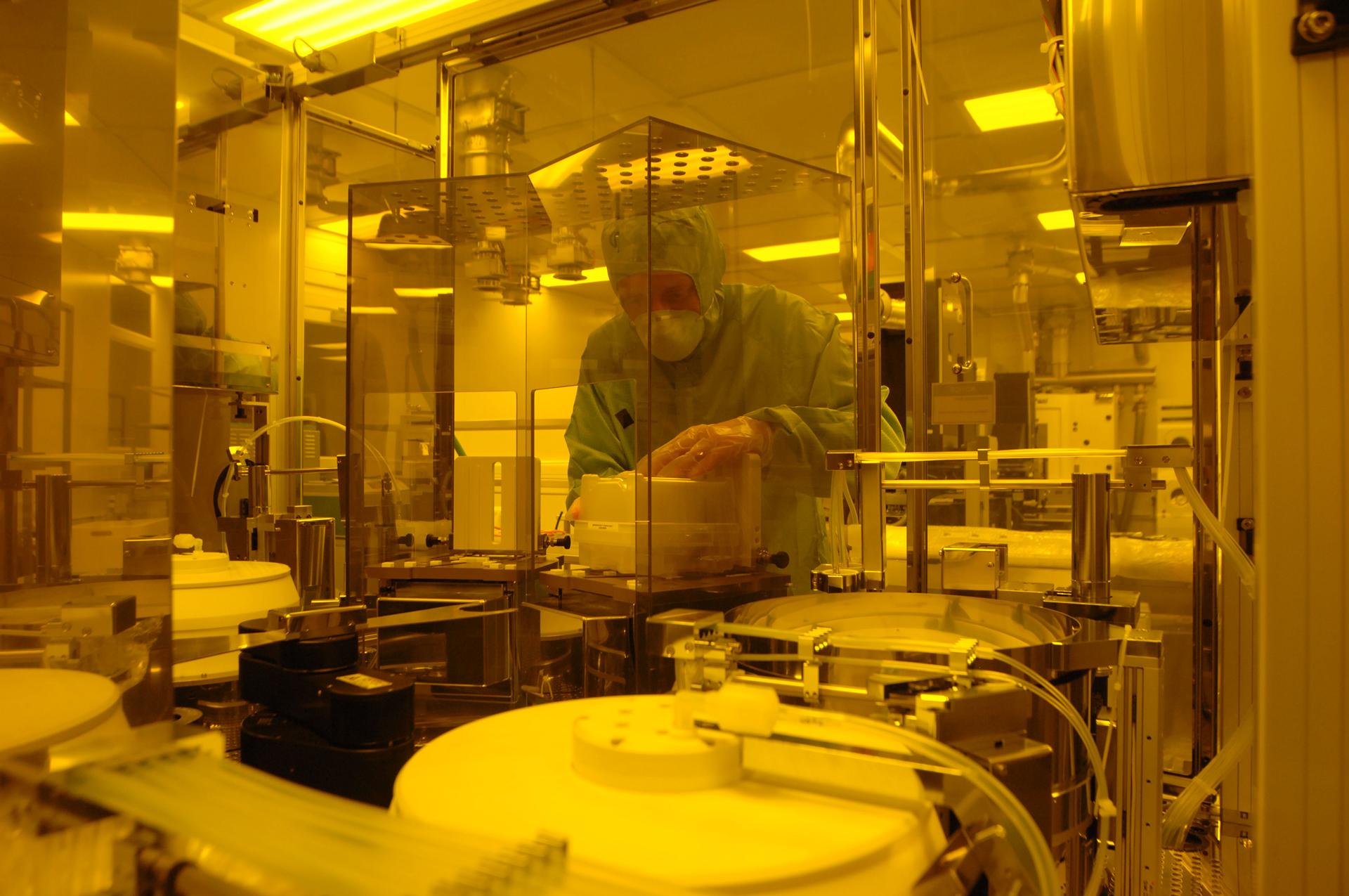
Our lab is located at the heart of the university of Southampton in the New Mountbatten Building, which opened in October 2008 and is one of Europe’s leading multidisciplinary state-of-the-art cleanroom complexes. The building provides flexible research space for nanotechnology and photonics nanofabrication.
Fabrication capabilities:
The ground floor cleanroom provides access to a wide range of tools and measurement capabilities for the development of integrated photonic devices. The pilot line enable the fabrication of individual samples and wafers from 3″ to 8″, with standard CMOS tools for lithography (ebeam, stepper and contact), etch(ICP, RIE), deposition (ebeam, CVD, sputtering), anneal (RTA, furnace) and CMP.
Packaging capabilities are also available with tools such as flip chip and wire bonders.

Our measurement capabilities cover optical, electrical and RF.
Optical measurements:
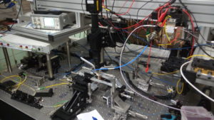
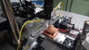
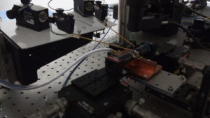
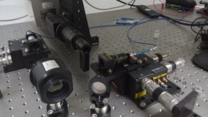
Multiple tuneable lasers enable the test of devices using grating (top down) or butt (end facet) coupling methods. The optical bandwidth covered are from ~400nm to ~2100nm, with polarisation control. Time resolved carrier lifetime and micro photoluminescence measurements in the near infrared and visible.
We also have detection and amplification capabilities (fibre amplifiers) for the entire range.
Electrical measurements:
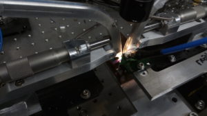
We have a range of computer driven electrical measurement capabilities for probing devices for low current and low/high voltage measurements.
This capability can be combined with optical measurements.
RF measurements:
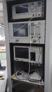
We have a set of instruments (VNA, PRBS, DCA (electrical and optical head), BERT) enabling data rate measurement up to 128Gb/s NRZ.
This capability enables characterization of modulator, and detector photonic devices
